← Back to Guides
build and installation of the Einstein TC01 TMS9929 Adapter
Version:
1
November 21, 2026
Page Chapter
3 WARNING AND LIABILITY NOTICE
4 INTRODUCTION
5 ITEMS REQUIRED IN ORDER TO PERFORM THE NECESSARY TASKS
6 ASSEMBLE THE TMS9929 BOARD
7 REMOVING THE MOTHERBOARD FROM THE CASE
9 THE DIFFICULT BIT
10 I HAVE DAMAGED A PAD OR TRACE WHAT DO I DO
14 FITTING THE TMS9929 UPGRADE BOARD
15 APPENDIX A - BILL OF MATERIALS
PLEASE NOTE - the following beforeproceeding:-
1) This project is notfor those unfamiliar with the use of a soldering iron
2) The informationprovided in this guide is for general informational purposes only.
3) The Einstein TC-01 iswell know for its fine traces, which can be easily damaged if you are not extremely careful.
4) By continuing to use this guide, you acknowledge and agree that you are doing so entirely at your own risk. You expressly agree to assume full responsibility for any outcomes, damages, or losses that may result from implementing the information provided.
INTRODUCTION
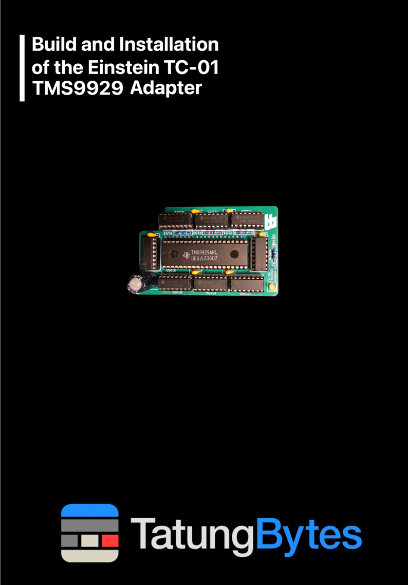
Recently the Einstein TC-01 has received a whole host of new hardware expansion/upgrade boards created by the Board-Folk team. One such board, TheTMS9929 Adapter is particularly useful for those that need to replace their damaged TMS9129 or are building the new Einstein Motherboards and experiencing difficulty obtaining the TMS9129.
This board effectively which replaces the need for the TMS9129 chip,but does requires a different type of RAM which needs fitting to the adapter.This is due to the motherboard ram being incompatible with the TMS9929 Chip.
This transformation is performed via the removal of the TC-01’s TMS9128VDP (Video Display Processor) and installation of a socket, the assembly of theTMS9929 board and its installation. Full details of everything involved in theimplementation of this board are covered in detail within this document and itis recommended that you read fully before commencing with this project.
It should be noted that this document was created by myself after the successful implementation of this solution on twoTC-01’s but that is not to say I had no issues at all, the fact is that I did damage one of the traces on one of the boards - but I easily rectified that and both Einstein work perfectly. I mention this mainly to emphasise that performing this upgrade is very possible but the utmost care must be taken not to damage your machine.
Upon completion of this project you will be presented with an EinsteinTC-01 that performs exactly as expected and still uses the external RGB port.
The Board-Folk Team’s Github page, featuring this and other EinsteinTC-01 upgrades can be found here:-
https://github.com/Board-Folk/Einstein-TC-01/tree/main/Expansions
ITEMS REQUIRED INORDER TO PERFORM THE NECESSARY TASKS
1. A small sharp pair of wire cutters
2. A decent soldering iron
3. A Solder Sucker
4. Flux
5. A large amount of narrow solder wick.
6. An anti-static soldering mat on which towork
7. An anti-static Wrist Strap which should beused in order to avoid damaging the chips you need to handle.
8. Some isopropyl alcohol (IPA) and Cotton buds or isopropylalcohol (IPA) wipes
9. A Blank TMS9929 Board - the Gerbers forwhich can be found here :-
https://github.com/Board-Folk/Einstein-TC-01/tree/main/Expansions/TMSAdapterTC01
and these can be used to order the blank boards fromsuppliers such as PCBWAY, JLCPCB,Etc
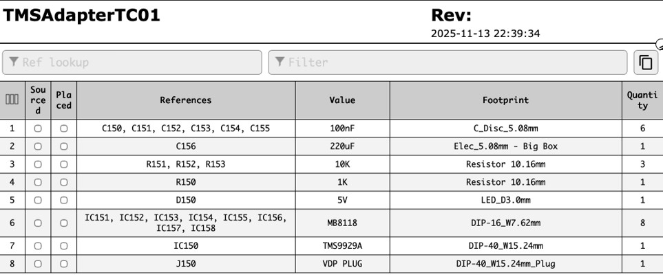
10. The Bill of Materials - listing all theparts needed to build the board is also available on the site above and In Appendix A of this document.
ASSEMBLE THE TMS9929BOARD
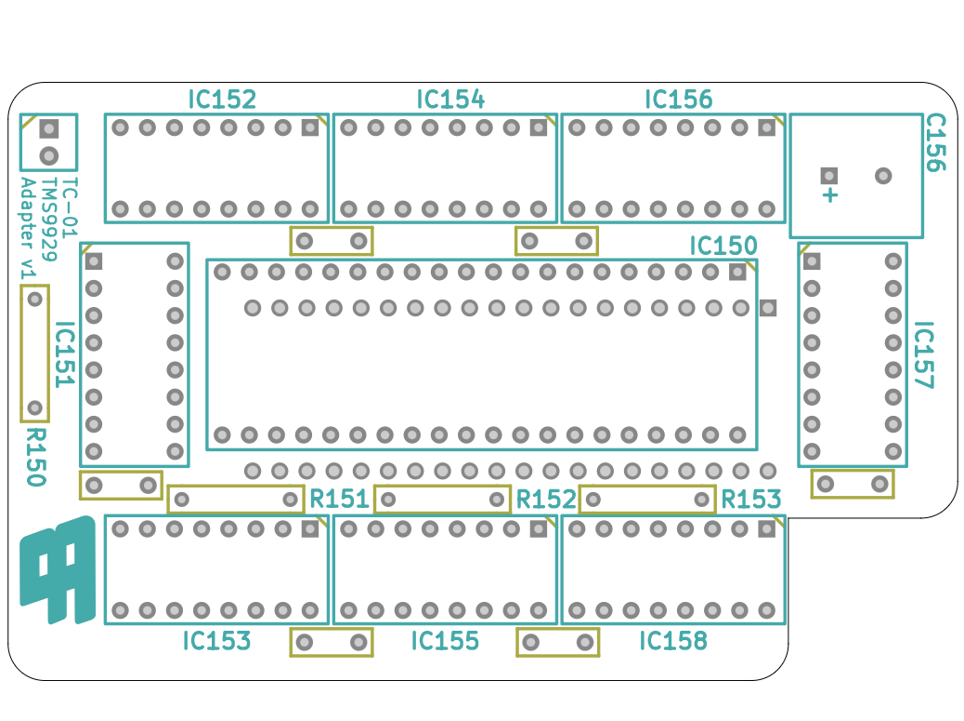
1. Using the parts you purchased (as listed on the BOM Bill of Materials),your Anti-Static Mat, Anti-Static Wrist strap, Soldering Iron, Solder, Flux,the Bill of Materials and the Schematic below, assemble your board. To avoid any issues with seating of chips, etc I would strongly suggest that you fit Dual Wipe DIP sockets for the memory and VDP chips.
2. When finished use the isopropyl alcohol (IPA) and Cotton buds or isopropyl alcohol (IPA) wipes toclean off the Flux.
REMOVING THEMOTHERBOARD FROM THE CASE
1. Turnoff your machine and disconnect all cables.
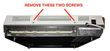
2. Remove the two screws on the back of your case and then from the rear lift the lid of the case, remove it and place it somewhere safe.
3. have access to the internals of the case and can clearly see all the screws holding the motherboard in place, but before you start removing them, you need to remove the Power supply.
To do this you need to look at the gap between your Disk Drive and Power Supply.
You will see two screws that need to be removed. Once removed the metal plate they were holding in place can be removed and the Power supply simply lifted out.
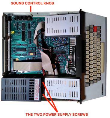
For those with bigger hands, you may find it useful to remove the primary disk drive from its cage. This will then give you much easier access to the two screws.
In order to remove the drive simply undo the four retaining screws, then slide the drive back, tilt it to an appropriate angle and then it can be removed from the cage.
NOTE: if you remove the cables from the back of the drive during this process, make sure you remember the way they were connected, as you will need to replace them correctly on completion of the project.
4. If you have a second drive installed you must remove this fromits cage as well.
5. Now you can go ahead and remove all the screws from the motherboard.
6. The next part is I am afraid never simple, by carefully jiggling the motherboard, slightly lifting on the Power supply side and a great deal of patience, remove the motherboard from the case.
Depending on your Einstein - you may be able to remove the volume control knob on the right side of your case, to provide more wiggle room.
REMINDER:-
1) This project is not for those unfamiliar with the use of a soldering iron.
2) The information provided in this guide is for general informational purposes only.
3) The Einstein TC-01 iswell know for its fine traces, which can be easily damaged if you are not extremely careful.
4) By continuing to use this guide, you acknowledge and agree that you are doing so entirely at your own risk. You expressly agree to assume full responsibility for any outcomes, damages, or losses that may result from implementing the information provided.
THE DIFFICULT BIT
Its now time to work on the motherboard, so for everything you have done was in preparation for this section and this is the part, where silly mistake scan ruin your Einsteins motherboard - so for the third and last time:-
REMINDER:-
1) This project is not for those unfamiliar with the use of a soldering iron
2) The information provided in this guide is for general informational purposes only.
3) The Einstein TC-01 iswell know for its fine traces, which can be easily damaged if you are not extremely careful.
4) By continuing to use this guide, you acknowledge and agree that you are doing so entirely at your own risk. You expressly agree to assume full responsibility for any outcomes, damages, or losses that may result from implementing the information provided.
Assuming you have decided to proceed, now comes the hard part of theproject, you need to remove the VDP and Voltage Regulator (both of which are shown in the picture below).
I find the following methods of extraction to be the easiest:-
The destructive but easy option, cut the chip away from all its pins (this should be done at the top of the pin, where it connects to the chip itself) using wire cutters. Then you can carefully heat the solder foreach pin, one at a time (on the bottom of the board), whilst using tweezers to remove the pin (from the top of the board) -
DO NOT USE EXCESSIVE FORCE - wait for the solder to melt so that the pin
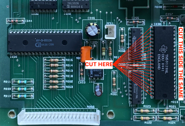
a. removes with no force or you will damage your board.
Pros = easier, quicker, less risk of motherboard damage.
Cons= you have destroyed your current VDP chip and theres no turning back now.
b. The Careful non Destructive option, placing plenty of flux on the solder of each pin of the chip, use your solder wick to remove all the solder to the point where you can gently get the chip out in one piece.
Pros=Chip intact.
Cons=any excessive pressure on the chip your trying to remove and you risk damaging the connector on the motherboard, its very time consuming and if you cause damage to your motherboard you will definitely regret it.
From my comments you can see I nearly always go for option “a” as I prefer to ensure the safety of my motherboard over all else but the choice is of course yours.
With the parts safely removed you can now install the the socket where the VDP was located and fit the Traco TSR 1-2450 Voltage Regulator. Be careful to ensure you install the Traco the correct way round.
I HAVE DAMAGED A PAD OR TRACE WHAT DO I DO
Without doubt this is not good news, but there are two things to keep in mind at this point, firstly, the fact that you now have a problem is not necessarily down to you doing something wrong, these machines are old and as such are prone to failure when modifications are made. Secondly, there is no need for panic, there are ways and means to repair the damage done. That said not ever issue will be repairable but most hopefully will be.
Although you were warned of the potential for damage earlier in this document, it was never my intention to leave those with issues high and dry, far from it, I will now attempt to explain what I did when I damaged one of my boards, in a way that I hope will help you resolve your problem
FIRSTLY AN EXPLANATION
Ok lets first of all explain what affect the lifting or removal of apad or damaging a trace has and why its such a problem.
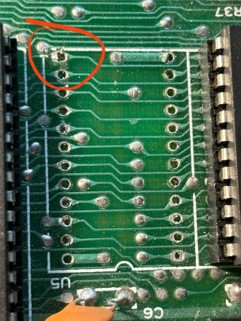
From the example picture shown on the right we can see that one pad has lifted which means soldering anything here is impossible. You can also see the traces going to these pads, perhaps its one of these you have damaged. The problem in both cases is the same - there are now parts of your computer that can no longer communicate with other parts.
The bottom line is, you have damaged your computer and now have no alternative, you have to fix this before you can proceed
THE REPAIR METHOD
Now we have to undertake the repair, which in my case was achieved byusing the Motherboard VIA’s.
AN INTRODUCTION TO VIA’s
On the Einstein’s motherboard, there are things called VIA’s, consisting of a small drilled hole in the circuit board these are used to connect electrical signals between the different layers of the circuit board. Basically the Via acts as a vertical bridge allowing traces to pass power and signals across the board.
For my purpose the Via’s provided excellent connection points, which I used to solve my problem.
LETS GET STARTED
First place your motherboard upside down and starting at the point of the problem carefully follow the trace leading up to and/or from the issue. In the example picture (not an Einstein) on the next page these are very clear to see.
The Trace between both the red and both the blue arrows is obvious -the silver pad is most likely what you have damaged but you may have damaged a trace, either way the repair is the same.
If you look closely at the silver pad of the blue arrow - you can clearly see there is a trace going both to the second blue arrow (The Via) and another leaving the same silver pad which (in the example pictures goes to one of the silver edge connectors in the top right hand corner).
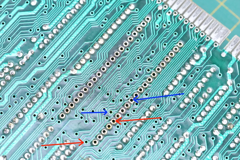
If you have damaged the trace between the pad and the VIA - Relax you need do nothing.
if you have damaged the trace leading to another component - you need to use some of the 30 Gauge PVC Hook up Wire you used earlier to solder a connection between the silver pad and its destination (in the example picture this would be the edge connector pad) - effectively your building a bridge over the damage.
Now at this point I need to add there is another fix you can/may need to perform instead -especially if the distance between the pad and the traces destination is quite far apart (more than two to three centimetres - because the longer the wire the more chance the fix wont work, due to degradation of the signal).
This solution follows the same logic, but this time you are going to scratch some of the trace away on the other side of the damage and then solder a wire (Bridge) from the pad to the trace you have just revealed - Same process, just a little harder to perform, especially if the trace you are going to is narrow and close to other traces.
Once performed you now need to use a Multi-Meter, set it to continuity,and check that the two points are indeed connected. If so and if you were careful not to damage anything else in the process, you have quite likely just fixed that problem.
If you have lifted or damaged a Pad - you now need to solder some of the 30 Gauge PVC Hook up Wire you used earlier between the pin protruding through the hole (where the pad was) and the VIA - again, be careful, take your time and when complete use a multi-meter, set it to continuity and test the connection from the via to the top of the pin protruding through the hole. If all is okay then you have quite likely just fixed that problem.
If you have lifted a pad and the trace going to it - then use the same technique but now youneed to go from the VIA to the protruding pin and from the protruding pin to the traces destination or trace that you have revealed.
Once performed you now need to use a Multi-Meter, set it to continuity,and check that the three points are indeed connected. If so and if you werecareful not to damage anything else in the process, you have quite likely justfixed that problem.
When you believe you have repaired your damage If you have a workingTMS9129 chip, plug it into the newly installed socket and then see if the computer functions as it should. If you (like me) destroyed the TMS9129 chip during the removal process, you will need to wait until completion of the project before you can test it.
Should any fix, fail the test, you need to go back and look for any other damage, retest your connections, etc, fix anything you find and retest. If the machine is still not working, then im afraid you now need to seek professional help.
FITTING THE TMS9929 UPGRADE BOARD
Carefully line up the pins on the bottom of the TMS9929 Board with the socket you recently installed, make sue you line up the pins perfectly, missalignment of the pins with the socket can cause damage to your computer and/or damage the pins on the adapter board meaning you will have to redo part of the board.
When your happy, turn the machine on and if everything has been done properly you will be presented with the normal Einstein TC-01 boot screen.
If for some reason the machine isnt working, check all your soldering, the alignment of the pins and that no pins have been bent or broken of, then retest.
Appendix A - Bill of Materials
This form is protected by reCAPTCHA, and the Google Privacy Policy and Terms of Service apply.
