module
16
.png)
Every character you have printed went through RST 8. Someone else's code
worked out which pixels to change, and you never saw it happen.
This section is where that stops. You are going to put a shape on the screen that you designed, in a colour you chose, without asking the ROM for anything - and then show the same shape in a second place for the cost of one byte.
That last part is the whole trick behind tile-based games, and by the end of this section you will have done it.
S15 established the shape of the problem: the picture lives in the VDP's own memory, and the Z80 cannot address it. Everything goes through two ports.
Ports are a part of the Z80 you have not used yet. They are a second, much smaller numbered space - nothing to do with memory - used for talking to hardware. Two instructions reach it:
        OUT (9),A       ; send what is in A to port 9
        IN  A,(9)       ; read port 9 into A
Only A can carry the byte, which is one more reason it is the busiest
register you have.
On the Einstein:
VRAM holds 16K, so an address needs fourteen bits, and a port carries eight. So an address goes in two halves, both to port 9:
First, the low eight bits of the address.
Then a byte made of three things: bit 7 clear, meaning you are addressing VRAM rather than a register; bit 6 set, meaning you intend to write; and in the bottom six bits, the top six bits of the address.
Bit 6 set is 40h, so that second byte is always 40h plus the high part of
the address:
        LD A,<low byte of address>
        OUT (9),A
        LD A,<40h + high part>
        OUT (9),A
        ; now every byte you send to port 8 goes into VRAM, one after another
The VDP keeps count. After the two setup bytes, each byte you send to port 8 lands at the next address along, so a run of data needs the address only once.
Address 0000. Low byte 0. High part 0. So 0 then 40h.
Address 1800. Low byte 0. The high part is 18h. So 0 then
40h + 18h = 58h.
Address 3B00. Low byte 0. The high part is 3Bh. So 0 then
40h + 3Bh = 7Bh.
The pattern never changes: low byte, then 40h plus the top six bits. In
hex it is barely arithmetic - 1800 becomes 58, 3B00 becomes 7B, and
the low byte is just the low byte.
S15 laid out the four regions. Three of them matter now.
| VRAM | What it holds |
|---|---|
0000-07FF |
Patterns - the shapes, 8 bytes each |
2000-27FF |
Colours - two per pattern row |
3800-3AFF |
The name table - which pattern each cell shows |
A cell on screen is 8 x 8 pixels, and there are 32 across and 24 down. To make a cell show something you need all three: a shape, its colours, and an entry in the name table pointing at it.
One limit for this section. Those addresses are right for cells in the top eight rows of the screen. Rows lower down read their patterns from somewhere else, for a reason that needs a section of its own. Stay in the top third for now and everything here works.
A pattern is eight bytes, one per row, one bit per pixel. A 1 shows in one colour and a 0 in the other.
So draw it on squared paper and read off the rows:
        . . . # # . . .        00011000
        . . # # # # . .        00111100
        . # # # # # # .        01111110
        # # # # # # # #        11111111
        # # # # # # # #        11111111
        . # # # # # # .        01111110
        . . # # # # . .        00111100
        . . . # # . . .        00011000
And you can write it in binary, which keeps the picture visible in your source:
shape:  DEFB 00011000b
        DEFB 00111100b
        DEFB 01111110b
        DEFB 11111111b
        DEFB 11111111b
        DEFB 01111110b
        DEFB 00111100b
        DEFB 00011000b
That is a diamond, and you can see that it is a diamond, which you cannot with
18h, 3Ch, 7Eh, FFh. This is the one place in the whole course where binary
literals earn their keep.
Here is the thing that makes this section easy, and it is worth understanding rather than just copying.
Right now the name table is a list of ascending numbers. Cell 0 shows pattern 0, cell 1 shows pattern 1, cell 34 shows pattern 34, all the way up. That is what makes MOS's screen a bitmap - every cell has a private pattern, so changing a pattern changes exactly one cell.
Which means you do not need to touch the name table to see your shape. Overwrite pattern 34 and cell 34 changes. Cell 34 is row 1, column 2, counting from zero - a blank part of the boot screen.
The cell at row r, column c is cell number r * 32 + c, and pattern n
lives at n * 8. So pattern 34 is at 34 * 8 = 272 = 0110h.
A pattern's two colours do not come from register 7. They come from the
colour table, laid out exactly like the patterns - eight bytes per pattern,
one per row - starting at 2000.
Each byte is two nibbles. The high nibble colours the 1 bits of that row, the
low nibble colours the 0 bits. So 90h means the shape is colour 9, light
red, and everything around it is colour 0.
Colour 0 is transparent, not black. Where a pattern is transparent you see straight through to the backdrop, which is the blue the screen already is.
So pattern 34's colours go at 2000 + 272 = 2110h.
        ORG 256

        ; --- the shape, into pattern 34
        LD A,10h        ; low byte of 0110h
        OUT (9),A
        LD A,41h        ; 40h + 01h
        OUT (9),A

        LD HL,shape
        LD B,8
send:   LD A,(HL)
        OUT (8),A
        INC HL
        DEC B
        JR NZ,send

        ; --- its colours, into the colour table
        LD A,10h        ; low byte of 2110h
        OUT (9),A
        LD A,61h        ; 40h + 21h
        OUT (9),A
        LD A,90h        ; light red shape, transparent around it
        LD B,8
col:    OUT (8),A
        DEC B
        JR NZ,col

        ; --- and show the same pattern in a second cell
        LD A,24h        ; low byte of 3824h - cell 36
        OUT (9),A
        LD A,78h        ; 40h + 38h
        OUT (9),A
        LD A,34         ; cell 36 now uses pattern 34
        OUT (8),A

        RET

shape:  DEFB 00011000b
        DEFB 00111100b
        DEFB 01111110b
        DEFB 11111111b
        DEFB 11111111b
        DEFB 01111110b
        DEFB 00111100b
        DEFB 00011000b
What you should see
Two light red diamonds, side by side with a gap between them, on the second row of the screen. The boot text is untouched.
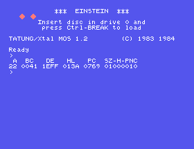
Notice how the pattern was sent: the address once, then eight bytes in a loop,
using the same LD A,(HL) / INC HL walk from S11. The VDP advanced its own
address each time.
The second diamond is the important one.
You wrote the shape once. Then one byte into the name table - LD A,34 -
made a second cell show it. Not a copy: the same eight bytes, displayed twice.
Write 34 into thirty more name table entries and you get thirty more
diamonds, at no cost in memory and almost none in time.
That is a tile, and it is why tile-based games can redraw a whole screen inside a single frame. A screen is not a picture; it is a list of which shape goes where, and the shapes are defined once.
Compare it with what you have been doing. Printing a character means the ROM computing pixel addresses and writing eight bytes per character. Placing a tile means writing one byte.
LD A,34 to LD A,35. The second diamond does not move - it
disappears. Work out what cell 36 is showing instead, and why "nothing" is
the wrong answer. Then try LD A,160, which is the pattern belonging to the
cell at row 5, column 0, and see what turns up in cell 36 - including what
colour it arrives in.24h to 25h. Which cell
changes now?90h to F0h in the colour write. What colour are the diamonds, and
what happened to the space around them?90h to 94h. Both nibbles now name a real colour, and yet nothing
on screen changes at all. Colour 4 is dark blue - look at what the screen
behind your diamond already is, and the reason will arrive. Then try 9Fh
and you will see the low nibble doing its job.3800 + 300 - which is in row 9.
The diamond does not appear, and you get a blank gap in the register line
instead where that cell should have text. Neither is a mistake in your
arithmetic, and the next section is about why.16.1 - Your own shape. Design something on an 8 x 8 grid - an arrow, a letter, a spaceship - and put it on screen. Write it in binary so you can read it back.
16.2 - A row of them. Show your shape across a whole row of the screen by
writing its pattern number into consecutive name table entries. One address
setup and a loop of OUT (8),A will do it, since the VDP advances the address
for you.
16.3 - Two shapes. Define a second pattern in a different pattern number, give it a different colour, and put both on screen. Then alternate them along a row.
16.4 - A striped cell. Make a pattern where every row is 10101010b and
give it a colour byte with two different nibbles. Look closely at the result
and explain which nibble coloured which pixels.
16.5 - Find a letter in the pattern table. Pick a cell on screen that
contains part of a letter - row 5, column 0 is the T of TATUNG - work out
its pattern address, and read the eight bytes back. Print each as eight
characters, a # for a 1 bit and a . for a 0, one row per line. The letter
will be looking back at you. That is the bitmap, and there is no clearer way
to see it.
Testing one bit at a time sounds like it needs an instruction you have not
met, and it does not. CP 128 tells you whether the top bit is set, and
ADD A,A from S14 moves the next bit up into that position. Eight of each and
you have the row. Expect a stray mark or two down the right-hand edge as well:
a cell is eight pixels wide and the text is not, so the cell holds a sliver of
the character next door.
16.6 - Read it back the short way. The datasheet says the second address
byte is 00h rather than 40h for a read. Set up a read address, use
IN A,(8), and fetch one of your own pattern bytes back. Check it against
what you wrote. If what comes back is not what went in, put a short do-nothing
loop between the address setup and the IN and try again: the VDP may need a
moment before the data is there.
| What you see | What it means |
|---|---|
| Nothing changes at all | The second address byte. It needs 40h added for a write - without it the VDP is set up to read. |
| The display corrupts wildly | Bit 7 set in the second byte, which makes it a register write instead. Keep it under 80h. |
| The shape appears somewhere unexpected | Pattern n is at n x 8, not at n. And cell r,c is r * 32 + c - 32 cells per row, not 40, even though text is 40 columns. |
| The shape is invisible but the cell went blank | Both colour nibbles the same, or both transparent. Try 90h. |
| A shape in the lower two thirds of the screen never appears | The pattern banks. Next section. |
| Text stops looking right afterwards | You overwrote a pattern that MOS was using for a character's pixels. Harmless: the cell repairs itself the next time MOS prints a character there, so it clears as soon as the screen scrolls. |
OUT (n),A sends a byte to a port; IN A,(n) reads one. Only A can carry
it.40h plus the top six bits. The
address then advances by itself for every byte you send to port 8.n * 8.2000 + n * 8 - high nibble for the 1 bits,
low nibble for the 0 bits. Colour 0 is transparent. Register 7 does not do
this.3800 says which pattern each cell shows. Cell r,c is
entry r * 32 + c.S17. A screen of your own. Your diamonds are sitting on a screen that still belongs to MOS, and a shape in the lower two thirds will not appear at all. Next you find out why, clear all three tables properly, and build a screen that is entirely yours - which means giving up the ROM's text output for good.
This form is protected by reCAPTCHA, and the Google Privacy Policy and Terms of Service apply.
